【[C5SOC】TERASIC友晶 Cyclone V SoC Development Kit and S
- 产品型号: C5SOC
- 产品品牌: TERASIC友晶科技/Intel FPGA
- 产品规格:
- 产品价格: 16155
- 咨询热线:027-87538900
The Altera® Cyclone® V SoC Development Kit offers a quick and simple approach to develop custom ARM® processor-based SOC designs accompanied by Altera’s low-power, low-cost Cyclone V FPGA fabric. This kit supports a wide range of functions, such as:
- Processor and FPGA prototyping and power measurement
- Industrial networking protocols
- Motor control applications*
- Acceleration of image- and video-processing applications*
- PCI Express® (PCIe®) x4 lane with ~1,000 MBps transfer rate (endpoint or rootport)
*Application-specific daughtercards, available separately, supporting a wide range of I/O and interface standards.
Featured devices
- Cyclone V SX SoC—5CSXFC6D6F31C6N (SoC)
- MAX® V CPLD—5M2210ZF256C4N (system controller)
- MAX II CPLD—EPM570GF100 (embedded USB-BlasterTM II cable)
FPGA configuration sources
- Embedded USB-Blaster II (JTAG) cable
- EPCQ flash (PFL)
- Hard processor system (HPS)
FPGA memory
- 1 GB DDR3 SDRAM (32 bit)
FPGA I/O interfaces
- 2X 10/100 Ethernet PHYs (EtherCAT)
- PCIe Gen 1 x4 female connector
- Universal high-speed mezzanine card (HSMC)—x4 transceivers, x16 TX LVDS, x16 RX LVDS
- One serial digital interface (SDI) channel
- Four SMAs for one transceiver channel
- x4 push buttons
- x2 switches
- x4 LEDs
HPS boot sources
- 128 MB QSPI Flash
- Removable Micro-SD Card flash
- FPGA
HPS memory
- 1 GB DDR3 SDRAM (32 bit) with error correction code (ECC)
- 128 MB QSPI flash
- Micro-SD Card socket with 4 GB Micro-SD Card flash device
HPS I/O interfaces
- x1 USB 2.0 On-the-Go (OTG)
- x1 10/100/1000 Gigabit Ethernet (10GbE/100GbE/1000GbE)
- x1 CAN
- x1 UART (UART to USB bridge)
- x1 real-time clock (with battery backup)
- x1 two-line text LCD
- 1-/2-channel, 20 bit delta-sigma analog-to-digital converter (Linear Technology LTC2422)
- x4 push buttons
- x4 switches
- x4 LEDs
Clocking
- Four-output programmable clock generator for FPGA reference clock inputs
- 125 MHz LVDS oscillator for FPGA reference clock input
- 148.5 MHz LVDS programmable voltage-controlled crystal oscillator (VCXO) for FPGA reference clock input
- 50 MHz single-ended oscillator for FPGA and MAX V FPGA clock input
- 100 MHz single-ended oscillator for MAX V FPGA configuration clock input
- SMA input for HPS clock
Power
- Laptop DC input 14—20 V adapter
System monitoring circuit
- Power (voltage, current, wattage)
HSMC breakout board
HSMC loopback board
-
Mechanical
- Board dimensions—8.19” x 5.22”
- Cyclone V SX FPGA Development Kit software content
-
Design examples
- Board test system (BTS)*
- Golden System Reference Design with Board Update Portal web server
- Complete documentation
-
SoC Embedded Design Suite Subscription Edition
- ARM Development Studio 5 (DS-5™) Altera Edition Toolkit
- Hardware-to-software handoff tools
- Linux run-time software for application development
- SoC hardware libraries for firmware development
- Application examples
-
Free software supported by Quartus® II software v13.1, Web Edition
* Watch the video to learn more.
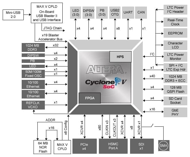
Schematic of the Cyclone V SX SoC Development Board

| No | 产品名称 | 售价(RMB) |
|---|---|---|
| 1. |
[C5SOC] Cyclone V SoC Development Kit and SoC Embedded Design Suite
产品编号: T0161
 重量: 3,500g 重量: 3,500g |
¥16,155 |
Documents
| 标题 | 版本 | 档案大小(KB) | 新增日期 | 下载 |
|---|---|---|---|---|
| Cyclone V SoC Development Kit User Guide (PDF) | 1.0 | 2015-03-19 |
 |
|
| Cyclone V SoC Development Board Reference Manual (PDF) | 1.0 | 2015-03-19 |
 |
CD-ROM
| 标题 | 版本 | 档案大小(KB) | 新增日期 | 下载 |
|---|---|---|---|---|
| Kit installation (EXE) (Windows) | 13.0.0.0 | 2015-03-19 |
 |
|
| Kit installation (EXE) (Linux) | 13.0.0.0 | 2015-03-19 |
 |
Software Guides


